
Your shopping cart is empty! Please select the type which you want.
This year, TSI, Samsung and Globalfoundries will produce 7Nm technology, the first generation 7Nm process will use the traditional DUV lithography process, the two generation 7Nm will be EUV photolithography process, is expected to be produced next year. When will the storage chip industry use EUV technology? In the light of Mei Guang, EUV lithography is not required by DRAM chip. It can't be used in the next few years. In the new generation process, they are checking 1Y nm memory chips by customers. In the future, there are 1Z, 1 alpha and 1 beta technology in the future.
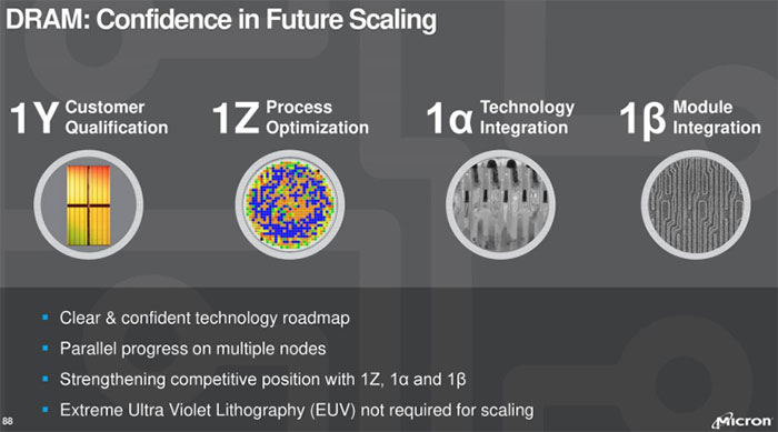
The memory industry will not need EUV lithography in the next few years.
Although the memory and CPU chips are integrated circuits, the manufacturing process has similarities, but the process is not the same, the CPU logic process has entered the 7Nm node this year, but the main main memory is 20nm, 18NM process, and 18NM belongs to the 1X nm node (16-19nm), and the 1Y nm is between the 14-16nm. Probably the 18NM is probably between the 14-16nm. 12 to 14nm. After that, Mei Guang proposed 1 alpha and 1 beta processes, and the corresponding XX nm is unknown.
Samsung is the first mass production 18NM technology, that is, the first to enter the 1X nm node, far ahead of other companies, mmm is now also starting to 1X nm technology, the next generation of 1Y nm technology has entered the customer verification stage, the next half of this year, the 1Z nm process node in the process optimization stage, 1 alpha and 1 beta processes, It is in different stages of research and development.
Mei Guang CEO Sanjay Mehrotra answered the relevant technical problems at the Bernstein annual strategic decision meeting. In the EUV photolithography process, he believed that the EUV lithography was not necessary in the manufacturing of DRAM chips, and it would not be used until the 1 and 1 beta processes.
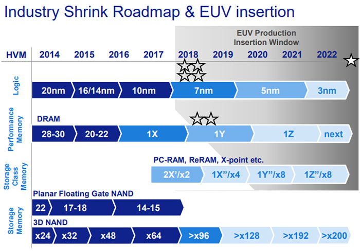
ASML has previously shared the progress of memory into the EUV process.
In memory technology, Mei Guang believes that 1 alpha and 1 beta technology still do not need EUV lithography process, but earlier ASML two years before the existence of the presence of 1Y nm nodes in the need to consider the EUV process, in fact, no, including Samsung, including the three big DRAM giants have not quickly entered the EUV node intention. Superenergy network
Contacto us Email: 1. Business Inquiries: winston@lhzzsz.com 2. Customer Support: xieyejia@lhzzsz.com Landline: +86-0755-82778656 Mobile: +86 15323875862 Main Contact: Mr. Xie Tencent QQ: 28836680 ( Mr. Xie ) Skype: live.c2a8ec407eb48aab WhatsApp: +86 15323875862 |
Free shipping for orders over $ 1000 USD Payment: |
Copyright © Lianhezhongzhi Technology ( Shenzhen ) Co., Ltd.

_782.png "支付方式1_00(10).png")